12-Layer Impedance Controlled HDI PCB on High Tg FR-4 Substrate
(Custom PCBs are tailored products; the images and specifications provided are for reference only.)
General Description
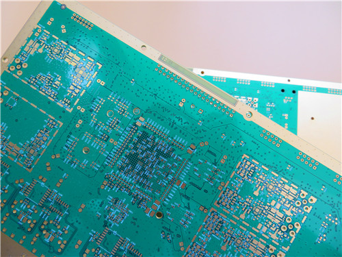
This impedance controlled PCB is built on FR-4 material with a Tg of 175°C, designed specifically for signal transmission. It features a 12-layer construction with a thickness of 2.0 mm. The board includes 2+N+2 HDI vias and is finished with white silkscreens (Taiyo) on a green solder mask (Taiyo) and immersion gold on pads. Both signal trace and differential pair impedances are carefully controlled. The base material is sourced from ITEQ, and the panels are fabricated per IPC 6012 Class 2 using provided Gerber data. Each shipment contains 20 boards.
Signal Trace Impedance Control
| Trace Layer | Trace Width (mil) | Trace Impedance (Ohm) | Precision | Reference Layer |
| Top Layer | 4 | 50 | ±10% | Mid-Layer 1 |
| L03, Mid-Layer 2 | 4 | 50 | ±10% | Mid-Layer 1 |
| L10, Mid-Layer 9 | 4 | 50 | ±10% | Mid-Layer 7, Mid-Layer 10 |
| Bottom Layer | 4 | 50 | ±10% | Mid-Layer 10 |
Differential Pairs Impedance Control
| Layer | Trace Width / Space (Mil) | Trace Impedance (Ohm) | Precision | Frequency (MHz) |
| Top Layer | 3.1 / 5.5 | 100 | ±10% | Mid-Layer 1 |
| Top Layer | 4.0 / 5.1 | 90 | ±10% | Mid-Layer 1 |
| L03, Mid-Layer 2 | 3.1 / 5.9 | 100 | ±10% | Mid-Layer 1, Mid-Layer 4 |
| L06, Mid-Layer 5 | 4.0 / 7.4 | 100 | ±10% | Mid-Layer 4, Mid-Layer 6 |
| L06, Mid-Layer 5 | 4.0 / 4.7 | 90 | ±10% | Mid-Layer 4, Mid-Layer 6 |
| L07, ,Mid-Layer 6 | 4.0 / 7.4 | 100 | ±10% | Mid-Layer 5, Mid-Layer 7 |
| L07, ,Mid-Layer 6 | 4.0 / 4.7 | 90 | ±10% | Mid-Layer 5, Mid-Layer 7 |
| L10, Mid-Layer 9 | 3.1 / 5.9 | 100 | ±10% | Mid-Layer 7, Mid-Layer 10 |
| Bottom Layer | 4.0 / 5.5 | 100 | ±10% | Mid-Layer 10 |
| Bottom Layer | 4.0 / 5.1 | 90 | ±10% | Mid-Layer 10 |
Features and Benefits
Lead-Free Assemblies: Maximum reflow temperature of 260°C.
Long Storage Life: Can be stored for over 1 year in a vacuum bag.
Enhanced Signal Speed: Improves transmission speed.
Custom Specifications: Manufactured according to specific requirements.
Timely Delivery: Quick and reliable shipping.
Compliance: UL recognized and RoHS Directive-compliant.
Prototype Capability: Supports prototype PCB production.
Applications
DSL Modems
Solar Battery Chargers
Vehicle Trackers
GPS Receivers
Wi-Fi Antennas
Bluetooth USB Hubs
USB Wireless Routers
SMS Modems
Multicoupler Antennas
Phone Systems
Parameter and data sheet
| PCB SIZE | 257 x 171.5mm=1PCS=1design |
| BOARD TYPE | Multilayer PCB |
| Number of Layers | 12 Layers |
| Surface Mount Components | YES |
| Through Hole Components | YES |
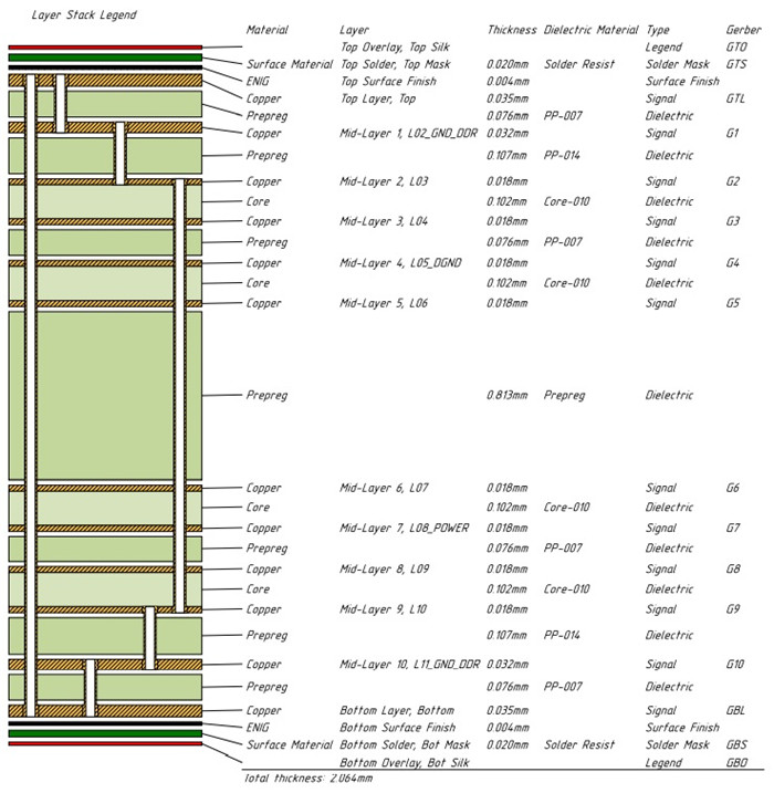
| LAYER STACKUP | copper ------- TOP 17um(1oz)+plate 25um |
| 130 um prepreg 1080 x 2 | |
| copper ------- L02 32um(1oz) | |
| 150um core FR-4 | |
| copper ------- L03 18um(0.5oz) | |
| 130 um prepreg 1080 x 2 | |
| copper ------- L04 18um(0.5oz) | |
| 150um core FR-4 | |
| copper ------- L05 18um(0.5oz) | |
| 130 um prepreg 1080 x 2 | |
| copper ------- L06 18um(0.5oz) | |
| 813um core FR-4 | |
| copper ------- L07 18um(0.5oz) | |
| 130 um prepreg 1080 x 2 | |
| copper ------- L08 18um(0.5oz) | |
| 150um core FR-4 | |
| copper ------- L09 18um(0.5oz) | |
| 130 um prepreg 1080 x 2 | |
| copper ------- L10 18um(0.5oz) | |
| 150um core FR-4 | |
| copper ------- L11 35um(1oz) | |
| 130 um prepreg 1080 x 2 | |
| copper ------- BOT 17um(0.5oz)+plate 25um | |
| TECHNOLOGY | |
| Minimum Trace and Space: | 4 mil / 4 mil |
| Minimum / Maximum Holes: | 0.25 mm / 3.0 mm |
| Number of Different Holes: | 26 |
| Number of Drill Holes: | 4013 |
| Number of Milled Slots: | 0 |
| Number of Internal Cutouts: | 0 |
| Impedance Control | Single Signal Impedance and Differential Pairs Impedance |
| BOARD MATERIAL | |
| Glass Epoxy: | FR-4, ITEQ IT-180, Tg>175℃, er<5.4 |
| Final foil external: | 1oz |
| Final foil internal: | 1oz |
| Final height of PCB: | 2.0mm ±10% |
| PLATING AND COATING | |
| Surface Finish | Immersion Gold (ENIG)( 2 µ" over 100 µ" nickel) |
| Solder Mask Apply To: | Top and Bottom, 12micon Minimum. |
| Solder Mask Color: | Green, PSR-2000GT600D, Taiyo supplied. |
| Solder Mask Type: | LPSM |
| CONTOUR/CUTTING | Routing |
| MARKING | |
| Side of Component Legend | TOP |
| Colour of Component Legend | White, IJR-4000 MW300, Taiyo Supplied. |
| Manufacturer Name or Logo: | Marked on the board in a conductor and leged FREE AREA |
| VIA | Plated Through Hole(PTH), Blind via L1-L2, L11-L12, Buried via L2-L3, L3-L10, L10-L11, via tented. Vin in pad under BGA package |
| FLAMIBILITY RATING | UL 94-V0 Approval MIN. |
| DIMENSION TOLERANCE | |
| Outline dimension: | 0.0059" (0.15mm) |
| Board plating: | 0.0030" (0.076mm) |
| Drill tolerance: | 0.002" (0.05mm) |
| TEST | 100% Electrical Test prior shipment |
| TYPE OF ARTWORK TO BE SUPPLIED | email file, Gerber RS-274-X, PCBDOC etc |
| SERVICE AREA | Worldwide, Globally. |
Impedance Control in PCB Design
The characteristic impedance of conductors on printed circuit boards is crucial for high-frequency circuit design. It's essential that the characteristic impedance aligns with the requirements of connected devices. Variations in impedance can lead to signal distortion, necessitating strict control during design.
Factors affecting impedance include copper track width and thickness, dielectric constant, pad thickness, and ground layer paths. Controlling impedance helps mitigate signal reflection and electromagnetic interference, ensuring the stability of PCB performance.
For precise calculations, refer to empirical formulas for micro-strip and strip line impedances on PCBs.
